Just like other larger electronics components, semiconductors undergo a lot of testing during the manufacturing process. One of these checks is wafer testing, which is also called circuit probing (CP) or electronic die sorting (EDS). This is a test wherein special test patterns are applied on individual integrated circuits on the semiconductor wafer. By doing so, functional defects on the wafer are detected.
Of course, that’s just an overview of what a wafer test is all about. For a more detailed look, let’s first check out the equipment used to conduct this test – a wafer prober.
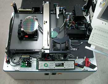
The Parts of a Wafer Prober
Admittedly, the structure of a wafer prober looks complicated at first. This machine consists of several parts—a tester, a measurement and stage travel part, and a wafer handling part. As the name suggests, the tester component transmits signals for testing the wafer. The signals are carried through cables onto the measurement and stage travel part, which opens and closes against the wafer handle part.
The travel mechanism itself is made of different parts. On the test head, a performance board and spring contact pin keeps a probe card secure. That probe card is tested against the wafer, which is vacuum-mounted on a wafer chuck. The wafer chuck, in turn, is mounted on a precision XY table that offers accurate movement.
This not only allows the prober to test the wafer down to its smallest section. It also allows for more automation, with the prober able to test wafers one after the other.
After the signals travel through the cable to the probe card and wafer, the signals are returned to the same path back to the tester. The tester then interprets those signals to check if there are defects.
The Importance of and Requirements for Wafer Testing
Now that you had a more nuanced look into the testing process, let’s see how wafer testing helps in improving semiconductor quality. First is in research and development (R&D), especially in testing wafer prototypes. Wafer testing allows manufacturers to evaluate the reliability of a prototype on top of analyzing potential defects.
That said, wafer probers for R&D may need to have additional features. These include a temperature control function for checking the prototype’s performance in different environments. There’s also a need to minimize – if not altogether eliminate – electrical noise and signal leakage. Manual probers may also be necessary for specialized tests.
Meanwhile, for mass production processes, wafer testing is usually deployed to evaluate the electrical testing of individual IC chips. Wafer probes for this kind of process need to have automated handling and position control to make testing more efficient. Reliability and easy maintenance are also sought-after characteristics for wafer probes in mass production testing. After all, manufacturers would want to minimize downtime in their facilities as much as possible.
As the above examples demonstrate, wafer testing isn’t just an essential step in semiconductor manufacturing. Choosing the right wafer probe—or assembling a customized rig—to conduct this test is also very important. With this test, manufacturers can guarantee that all their electronic products are in tip-top shape before being shipped and sold to consumers around the globe.