An Altera FPGA board is an incredible piece of technology capable of performing any unique function the designer chooses. However, working with an FPGA board for the first time can be a very daunting task. Understanding the basics of the FPGA design flow will help you get started on the right foot with your new Altera board.
The following guide will cover the basics steps involved in developing an FPGA device. The five steps of the design flow are:
- Design
- Compile
- Simulate
- Program
- Hardware Verify
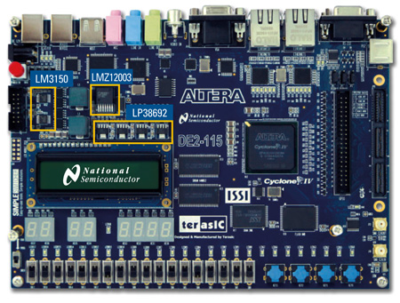
The information will assume that you know what an FPGA is and that you’ve installed the software that is compatible with your Altera FPGA board. In most cases, that will be the Altera Quartus II PLD design software or the newly named Intel Quartus. It also assumes you have properly installed the required drives and connected the Altera board to your computer.
- Design
In the design stage, you will create a schematic or use RTL code to implement the logic necessary for the board to function. The exact nature of that schematic or RTL will depend entirely on the intended function of the board.
If you are familiar with programming, then you have encountered the “hello world” concept before, which is where you create a very simple program that performs a simple function to help you learn the basics of the language. Often time, that program prints the words “Hello World” on the screen. When electronics are involved, the “Hello World” program generally involves causing an LED to blink and be influenced by some form of input. That’s a great place to start with your first Altera FPGA design.
To do this, you will need to create a new project in Altera Quartus. The process will be relatively the same if you are using an alternative program, but there may be some slight differences. Quartus includes a handy project wizard that will guide you through several steps, including naming the project, choosing a directory, and naming the top level design entry. You will need to select your Altera board from a list of available devices to finish creating the project.
The rest of this step will involve the specifics of the software you are using and the HDL programming language you are using. If you are already familiar with Verilog HDL, then creating the necessary .bdf file will be simple. If not, there are a lot of excellent learning materials available online. Many of them are available directly on the Xilinix FPGA website.
By the end of this step, you should have created a schematic or RTL that provides the necessary power to the pins and considers the input of some device, such as a switch, a clock, a potentiometer, or a sensor. Now it’s time to move further through the design flow with project compilation.
- Compile
The point of compiling the project is to convert the programming and schematics from the previous stage into a bitstream that the FPGA can actually use. You will most likely need to compile the previous project into a .sof file, which is an SRAM Object File. That file is then responsible for programming the FPGA once it is uploaded to the board. It is possible to compile as a different file type if you plan to store the programming in a different memory type, such as EEPROM or flash.
This process is very simple with the Quartus program. You choose “start Compilation” from the processing menu and then press the “play” button. A number of messages may pop up during the compilation process. Minor warnings are okay, but if any critical warnings appear then you will need to return to the previous stage and correct the area of the project that is causing the problem.
- Simulate
You could immediately upload the file to the FPGA board to program the device, but it is highly recommended that you simulate the program first. Simulation can help detect any serious errors that made it past the compiler. It can also prevent serious damage to an FPGA board that could be caused by those errors. Such damage is not a major concern when working with a project as small and simple as driving an LED, but it is a good practice to habit for when you begin working with larger projects.
There are a number of excellent FPGA simulation programs on the market. Simulation will generally fall into one of two categories. The first type is called timing simulation. This will determine if your project meets necessary timing constraints and will function on the particular Altera board you are using. The second type is called RTL simulation and it is used to verify that the code works properly in regards to the inputs and outputs of the board. You are advised to test your compiled program in both types of simulation environments before moving to the next stage.
- Program
Now that you have the necessary SRAM Object File it is time to upload it to the FPGA board and program the device. Once again, this stage will be very simple thanks to the Quartus software package. The .sof file that you compiled in stage 2 will be uploaded to the board via USB connection to the USB-Blaster circuitry. If your FPGA board does not come with USB blaster circuitry, then you will need to read the manual to determine exactly how to program the device. Once the board is powered on and the USB connection is made you can begin programming the device from the Quartus software.
- Hardware Verify
You have reached the final stage of the design process. This is where you verify that the original program works on the Altera board as intended. Exactly how the program works will depend on your specific project. Hopefully, your LED turns on and can be manipulated by some form of input. If it does not work, then you will need to return to stage one, identify the problem, and proceed through each stage until reach stage five again.
Understanding this simple design flow will help you as you move to larger and more complicated projects. The design flow rarely changes regardless of the complexity of the project.